The Flat Optics Revolution: Decoding DOE vs. Metalens for Future Tech
- IntelliGienic
- Nov 18, 2025
- 3 min read

Updated: Mar 25
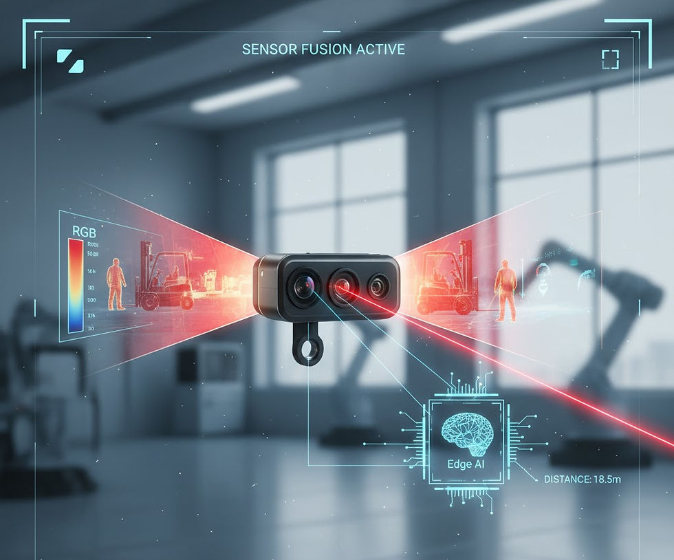
As AI Vision systems shrink, traditional refractive lenses—which rely on bulk material curvature to bend light—are hitting physical and integration limits. The transition to Flat Optics allows for high-performance sensing in a fraction of the Z-height. To navigate this shift, engineers must distinguish between two primary technologies: Diffractive Optical Elements (DOE) and Metalenses.

Diffractive Optical Elements (DOE): Micro-Scale Precision
DOE technology has been the industrial standard for beam shaping, splitting, and structured light (such as LiDAR and 3D sensing) for decades.
The Physics: DOEs operate on the principle of diffraction rather than refraction. The surface is etched with micro-structured relief patterns—essentially a series of discrete "steps." These steps shift the phase of the incident light wave, creating interference patterns that shape the output beam into specific patterns or dots.
The Scale: The feature sizes of a DOE are typically in the micron range. While the resulting component is significantly thinner than a standard curved lens, the functional structures are still large relative to the wavelength of light.
Manufacturing: They are produced using established semiconductor lithography and replication techniques like Nanoimprint Lithography (NIL), making them highly cost-effective for high-volume consumer electronics.
Metalenses: The Nano-Scale Frontier
Metalenses represent a fundamental shift in optical design, moving from micro-scale "steps" to sub-wavelength "meta-atoms."
The Physics: A Metalens uses a metasurface—an array of pillars, fins, or holes that are smaller than the wavelength of the light they are manipulating. These "meta-atoms" act as local phase-shifters. By varying the geometry and density of these nanostructures across the surface, a Metalens can provide a continuous phase shift, allowing for near-perfect wavefront control.
The Scale: The structures are in the nanometer (nm) range. For visible light applications (approx. 400–700 nm), the pillars feature sub-wavelength widths and are often only 500nm to 1,000nm tall. To put this in perspective, these active optical nanostructures are nearly 100 times thinner than a human hair, enabling extraordinary wavefront control within a drastically compressed footprint.
The Advantage: Metalenses can be designed to be nearly aberration-free and can achieve a much higher Numerical Aperture (NA) in a thinner profile than a DOE, making them ideal for high-resolution imaging.
Technical Comparison: DOE vs. Metalens
Feature | Diffractive Optical Elements (DOE) | Metalenses (Metasurfaces) |
Operational Scale | Micro-scale | Nano-scale |
Phase Modulation | Discrete Phase Steps | Continuous Phase Shift |
Light Interaction | Diffraction through bulk steps | Localized sub-wavelength scattering |
Design Flexibility | Best for pattern generation/splitting | Best for high-res imaging & aberration correction |
Efficiency | High (for specific diffraction orders) | Potentially higher across wider bandwidths |
Engineering Considerations for Integration
When selecting between these two flat-optic paths, the choice often comes down to the Wavelength and the Application:
Chromatic Aberration: Historically, both technologies struggle with chromatic aberration (color blurring). However, Metalenses offer more sophisticated "Achromatic" design potential through complex meta-atom geometry, whereas DOEs are typically optimized for single-wavelength laser sources (e.g., 850nm or 940nm IR).
Angle of Incidence: DOEs are highly sensitive to the angle of incoming light. Metalenses can be engineered to maintain performance over a wider Field of View (FOV), making them superior for compact camera modules and AR/VR headsets.
Mass Production: While DOEs are ready for mass production today due to mature etching and injection processes, Metalenses require advanced DUV (Deep Ultraviolet) lithography. This leverages 12-inch semiconductor foundry capacity, making them a premium choice for specialized, ultra-compact applications.
Conclusion: The Future of Vision Hardware
The "Flat Optics Revolution" isn't about one technology replacing the other; it’s about choosing the right scale for the task. Whether utilizing the micron-level reliability of a DOE for structured light or the nano-scale precision of a Metalens for imaging, the end goal remains the same: reducing the physical footprint of intelligence.

Comments